 Fraunhofer Institute for Manufacturing Engineering and Automation IPA
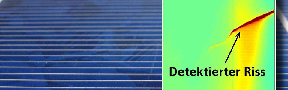
Detecting Micro Cracks, e.g. in Solar Cells
The sun is an almost inexhaustible supply of energy. In order to obtain electricity from sunlight effectively and sustainably, photovoltaic systems need to function efficiently over a long period of time. This is essentially determined by the process used to manufacture the solar cells. The silicon wafers are advanced along the production chain either by robot, conveyor or other handling method. The handling process subjects the silicon material to mechanical stress, possibly causing large or small cracks (so-called micro cracks) to be formed. These impair the function and longevity of solar cells.
For a solar cell manufacturing technology to succeed on the market and thus be profitable for the solar cell manufacturer, the solar cells produced and dispatched have to be in perfect condition. Therefore, before leaving the factory, solar cells have to be thoroughly checked for obvious external cracks or internal cracks.
At the start of the manufacturing process, cracks going right through the substrate can still be detected in transmitted light images. However, at the latest when the complete undersurface of the wafer is contacted with metal, this approach is no longer suitable. Instead, alternative methods, such as electroluminescence or thermography, are required.
Drawing on its extensive experience in industrial image-processing, Fraunhofer IPA has developed a system for inspecting finished solar cells. The inspection is based on the principle of heat flow thermography, which is increasingly becoming established as a non-destructive testing technology. Different surfaces of an object as well as structures near the surface can be evaluated for defects using this non-contact, non-destructive technique. The inspection system comprises the full image-processing chain, from image acquisition (heat stimulation, camera) through image analysis right up to its connection to a superior process control system. The combination of the active, inhomogeneous input of heat and a dynamic test arrangement is ideally suited for checking metallized wafers for the presence of micro cracks. It can be used on mono- as well as polycrystalline solar cells – just one of the advantages of the IPA method over other techniques. The newly-developed system is capable of identifying not only wide, easily-detectable cracks in the silicon layer but also cracks with widths < 20 µm at a typical production speed of 10 meters per minute. The IR-testing system is integrated directly at the level of the conveyor modules of the manufacturing system. The excellent image data also allows later automated analysis of the solar cells, classifying them as IO/NIO. The system meets cycle time requirements and the thermographic tests do not slow down the production process.