 Fraunhofer Institute for Manufacturing Engineering and Automation IPA
Flexible proximity sensor creates smart surfaces
Fraunhofer IPA has developed a proximity sensor made from silicone and carbon nanotubes (CNT) which detects objects and determines their position. The materials and printing process used mean that the sensor is extremely flexible, economical and can be used for large surfaces. Industry and research partners can use and further develop this innovation straight away.
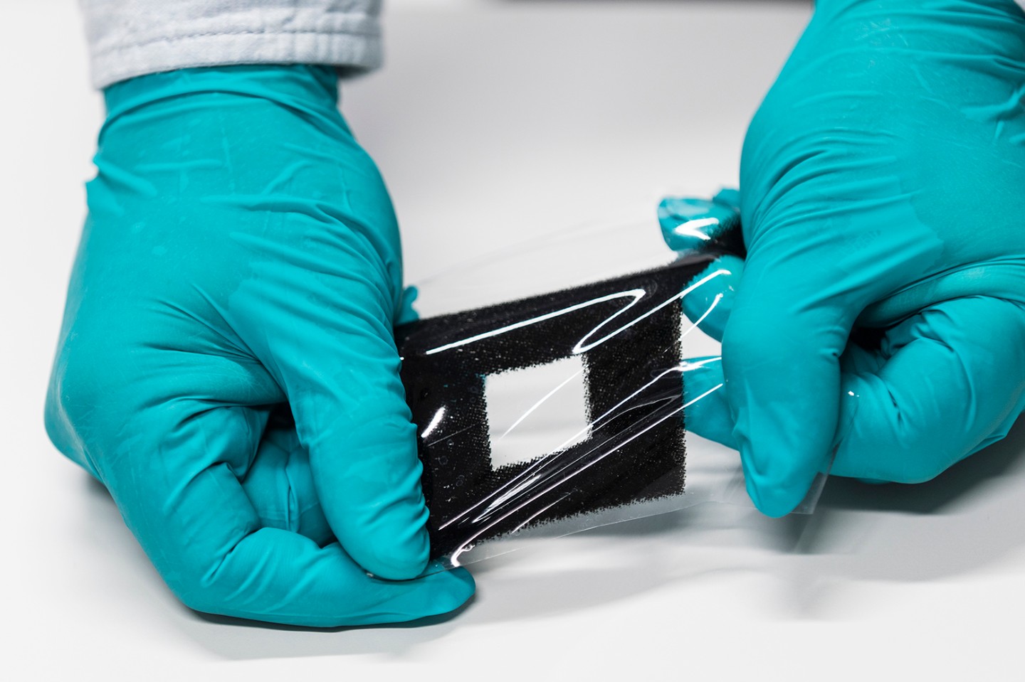
At first glance, the proximity sensor appears to be nothing special: a thin, elastic layer of silicone onto which black square surfaces are printed, but these areas are actually made up of countless microscopic carbon nanotubes which can locate humans and objects. Florian Bodny, a scientist at Fraunhofer IPA, explains: “The proximity sensor can detect anything which is electroconductive. When an object approaches, the electric field changes.” This can be observed when the sensor is connected to a testing device. Once connected, if a hand or a metal object is held above it then a light will turn on. If the surface is made up of several sensor elements, it detects both the object itself as well as its location.
Manufacturing costs under one euro
Scientists at Fraunhofer IPA used a combination of silicone and CNT in their sensor. It is constructed layer by layer, so a coat of silicone is followed by a silicone-CNT hybrid. Both materials are elastic and flexible, with a high degree of environmental stability. This means that the sensor can be applied across large surface areas. The experts decided to use screen printing for the manufacturing process. Bodny vouches for this method, saying that it is fast and can be done without any expensive or cumbersome preparations. Furthermore, he says that it is possible to print large surfaces and to manufacture the sensors in large quantities. “The sensor is easy to apply, is extremely versatile and is cheap to produce,” he explains.
Scientists at Fraunhofer IPA carried out a series of experiments to ascertain which parameters are important when it comes to detection accuracy. They discovered that the concentration of the active material had the biggest influence. The thickness of the layers was the second most important aspect, followed by the area of the sensor. Bodny explains: “To detect an object which is 8 mm away, for instance, three printed layers, a concentration of 1.5 m% and an area of 36cm² are needed.”
Seeking partners for application
The proximity sensor could be used for a variety of applications. It could conceivably be used as an artificial skin for robots. “For instance, service robots could reach out a hand if they sense a person nearby,” Bodny says. There are plenty of application areas in the “smart home” sector too, for instance in lights or doors which activate when they detect the presence of a person. Additionally, the sensor’s elasticity makes it well-suited for accident prevention, such as in PPE clothing. The scientists are also considering its use in medical engineering for exoskeletons. “The sensor is available right now. We are looking for industry and research partners who would like to test it and develop it further,” Bodny explains.
The proximity sensor is an example of printed electronics. This sector is generally used to create smart surfaces. Given the current trend of Industry 4.0, which sees objects being fitted with smart features and communicating with others as cyberphysical systems, sensors like these will be of increasing importance. In this respect, surfaces with proximity sensors can act as a human-machine interface.